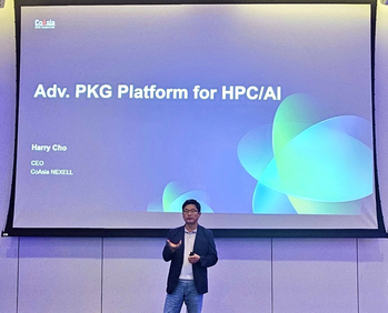
CoAsia Semi Presents Next-Generation Chiplet Platform ‘CoCs™’ and Advanced Packaging Roadmap at Samsung SAFE Forum
SANTA CLARA, Calif., [May 28, 2026] – CoAsia Semi today unveiled the latest roadmap for its next-generation chiplet packaging platform, ‘CoCs™ (CoAsia Chiplet Solution),’ at Samsung Foundry’s SAFE™ Forum 2026 held in Silicon Valley. Amid the rapid expansion of the AI and HPC markets and the growing limitations of large monolithic (big die) architectures, CoAsia Semi presented a next-generation chiplet solution designed to improve development efficiency while optimizing performance, yield, and power efficiency. CoAsia Semi’s CoCs™ is a platform that partitions a single chip into functional dies and applies optimized process technologies and packaging architectures to each die. By standardizing and modularizing chiplet architecture design and advanced packaging implementation, the platform enables faster and more reliable development of AI and HPC semiconductors tailored to customer requirements. The platform supports high-bandwidth memory solutions, including HBM3E, as well as the latest high-speed interfaces such as UCIe, PCIe, and SerDes. It is optimized for ultra-high-speed data processing and high-density integration required for next-generation AI and HPC semiconductors. CoAsia Semi stated that it has reduced development time and manufacturing costs by validating more than 200 SI/PI(Signal and Power Integrity) parameters during the pre-simulation stage and applying standardized methodologies across projects. At the forum, CoAsia Semi also unveiled its roadmap for 3D packaging solutions based on stacked SoC and memory dies, moving beyond conventional 2.3D/2.5D structures based on RDL and interposer technologies. Aligned with Samsung Foundry’s advanced process technologies, the company plans to progressively expand its portfolio of high-speed interface IPs—including LPDDR, MIPI, PCIe, and UCIe—as well as HBM platforms, while further advancing next-generation packaging architectures designed for AI and HPC applications. The company plans to complete sample validation for its 3D packaging solution in the second quarter and begin volume production in the third quarter. It is also pursuing sample-out of its 2.5D chiplet platform within the year. From a business perspective, CoAsia Semi is expanding its collaboration ecosystem with Samsung Foundry and leading global OSAT companies such as Amkor and ASE. The company has also established end-to-end execution capabilities backed by an integrated supply chain management system spanning interposer and substrate design, packaging partners, materials suppliers, and volume production. DS Shin, CEO of CoAsia Semi, said, “In the AI and HPC era, competitiveness increasingly depends not only on chip design capabilities, but also on advanced packaging and supply chain integration. Building on CoCs™, we will continue to strengthen our competitiveness in next-generation chiplet solutions within the Samsung SAFE ecosystem.” 정현식 기자packaging generation packaging platform packaging architectures packaging implementation
2026.05.28. 18:00